- 您现在的位置:买卖IC网 > Sheet目录3861 > PIC18F26K80-I/MM (Microchip Technology)MCU PIC 64KB FLASH 28QFN
PIC18F66K80 FAMILY
DS39977F-page 256
2010-2012 Microchip Technology Inc.
19.1
CCP Module Configuration
Each Capture/Compare/PWM module is associated
with a control register (generically, CCPxCON) and a
data register (CCPRx). The data register, in turn, is
comprised of two 8-bit registers: CCPRxL (low byte)
and CCPRxH (high byte). All registers are both
readable and writable.
19.1.1
CCP MODULES AND TIMER
RESOURCES
The CCP modules utilize Timers, 1 through 4, varying
with the selected mode. Various timers are available to
the CCP modules in Capture, Compare or PWM
modes, as shown in Table 19-1.
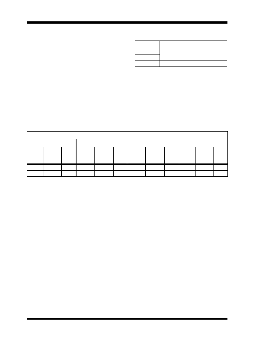
TABLE 19-1:
CCP MODE – TIMER
RESOURCE
The assignment of a particular timer to a module is
determined by the Timer to CCP enable bits in the
CCPTMRS register (see Register 19-2). All of the
modules may be active at once and may share the
same timer resource if they are configured to operate
in the same mode (Capture/Compare or PWM) at the
same time.
The CCPTMRS register selects the timers for CCP
modules, 2, 3, 4 and 5. The possible configurations are
shown in Table 19-2.
TABLE 19-2:
TIMER ASSIGNMENTS FOR CCP MODULES 2, 3, 4 AND 5
19.1.2
OPEN-DRAIN OUTPUT OPTION
When operating in Output mode (the Compare or PWM
modes), the drivers for the CCPx pins can be optionally
configured as open-drain outputs. This feature allows
the voltage level on the pin to be pulled to a higher level
through an external pull-up resistor and allows the
output to communicate with external circuits without the
need for additional level shifters.
The open-drain output option is controlled by the
CCPxOD bits (ODCON<6:2>). Setting the appropriate
bit configures the pin for the corresponding module for
open-drain operation.
CCP Mode
Timer Resource
Capture
Timer1 or Timer3
Compare
PWM
Timer2 or Timer4
CCPTMRS Register
CCP2
CCP3
CCP4
CCP5
C2TSEL
Capture/
Compare
Mode
PWM
Mode
C3TSEL
Capture/
Compare
Mode
PWM
Mode
C4TSEL
Capture/
Compare
Mode
PWM
Mode
C5TSEL
Capture/
Compare
Mode
PWM
Mode
0
TMR1
TMR2
0
TMR1
TMR2
0
TMR1
TMR2
00
TMR1
TMR2
1
TMR3
TMR4
1
TMR3
TMR4
1
TMR3
TMR4
01
TMR3
TMR4
发布紧急采购,3分钟左右您将得到回复。
相关PDF资料
PIC16C55-RC/P
IC MCU OTP 512X12 28DIP
SFW23R-2STE1
SFW23R-2STE1-FFC/FPC CONN
PIC24FJ64GA002-E/SS
IC PIC MCU FLASH 64K 28-SSOP
PIC18LF46K22-I/ML
IC PIC MCU 64KB FLASH 44QFN
PIC18F45K80-I/ML
MCU PIC 32KB FLASH 44QFN
PIC24F32KA302-I/ML
MCU 32KB FLASH 2KB RAM 28-QFN
PIC18LF45K80-I/ML
MCU PIC ECAN 32KBFLASH 44QFN
PIC18F4221-I/PT
IC PIC MCU FLASH 2KX16 44TQFP
相关代理商/技术参数
PIC18F26K80-I/SO
功能描述:8位微控制器 -MCU 64KB FL 4KBRM 16MIPS 12bit ADC CTMU RoHS:否 制造商:Silicon Labs 核心:8051 处理器系列:C8051F39x 数据总线宽度:8 bit 最大时钟频率:50 MHz 程序存储器大小:16 KB 数据 RAM 大小:1 KB 片上 ADC:Yes 工作电源电压:1.8 V to 3.6 V 工作温度范围:- 40 C to + 105 C 封装 / 箱体:QFN-20 安装风格:SMD/SMT
PIC18F26K80-I/SP
功能描述:8位微控制器 -MCU 64KB FL 4KBRM 16MIPS 12bit ADC CTMU RoHS:否 制造商:Silicon Labs 核心:8051 处理器系列:C8051F39x 数据总线宽度:8 bit 最大时钟频率:50 MHz 程序存储器大小:16 KB 数据 RAM 大小:1 KB 片上 ADC:Yes 工作电源电压:1.8 V to 3.6 V 工作温度范围:- 40 C to + 105 C 封装 / 箱体:QFN-20 安装风格:SMD/SMT
PIC18F26K80-I/SS
功能描述:8位微控制器 -MCU 64KB FL 4KBRM 16MIPS 12bit ADC CTMU RoHS:否 制造商:Silicon Labs 核心:8051 处理器系列:C8051F39x 数据总线宽度:8 bit 最大时钟频率:50 MHz 程序存储器大小:16 KB 数据 RAM 大小:1 KB 片上 ADC:Yes 工作电源电压:1.8 V to 3.6 V 工作温度范围:- 40 C to + 105 C 封装 / 箱体:QFN-20 安装风格:SMD/SMT
PIC18F26K80T-I/ML
功能描述:8位微控制器 -MCU 64KB FL 4KBRM 16MIPS 12bit ADC CTMU RoHS:否 制造商:Silicon Labs 核心:8051 处理器系列:C8051F39x 数据总线宽度:8 bit 最大时钟频率:50 MHz 程序存储器大小:16 KB 数据 RAM 大小:1 KB 片上 ADC:Yes 工作电源电压:1.8 V to 3.6 V 工作温度范围:- 40 C to + 105 C 封装 / 箱体:QFN-20 安装风格:SMD/SMT
PIC18F26K80T-I/MM
功能描述:8位微控制器 -MCU ECAN 64KB FL 4KBRM 16 MIPS 12b ADC CTMU RoHS:否 制造商:Silicon Labs 核心:8051 处理器系列:C8051F39x 数据总线宽度:8 bit 最大时钟频率:50 MHz 程序存储器大小:16 KB 数据 RAM 大小:1 KB 片上 ADC:Yes 工作电源电压:1.8 V to 3.6 V 工作温度范围:- 40 C to + 105 C 封装 / 箱体:QFN-20 安装风格:SMD/SMT
PIC18F26K80T-I/SO
功能描述:8位微控制器 -MCU 64KB FL 4KBRM 16MIPS 12bit ADC CTMU RoHS:否 制造商:Silicon Labs 核心:8051 处理器系列:C8051F39x 数据总线宽度:8 bit 最大时钟频率:50 MHz 程序存储器大小:16 KB 数据 RAM 大小:1 KB 片上 ADC:Yes 工作电源电压:1.8 V to 3.6 V 工作温度范围:- 40 C to + 105 C 封装 / 箱体:QFN-20 安装风格:SMD/SMT
PIC18F26K80T-I/SS
功能描述:8位微控制器 -MCU 64KB FL 4KBRM 16MIPS 12bit ADC CTMU RoHS:否 制造商:Silicon Labs 核心:8051 处理器系列:C8051F39x 数据总线宽度:8 bit 最大时钟频率:50 MHz 程序存储器大小:16 KB 数据 RAM 大小:1 KB 片上 ADC:Yes 工作电源电压:1.8 V to 3.6 V 工作温度范围:- 40 C to + 105 C 封装 / 箱体:QFN-20 安装风格:SMD/SMT
PIC18F27J13-I/ML
功能描述:8位微控制器 -MCU 128KB Flash 4KB RAM 12MIPS nanoWatt RoHS:否 制造商:Silicon Labs 核心:8051 处理器系列:C8051F39x 数据总线宽度:8 bit 最大时钟频率:50 MHz 程序存储器大小:16 KB 数据 RAM 大小:1 KB 片上 ADC:Yes 工作电源电压:1.8 V to 3.6 V 工作温度范围:- 40 C to + 105 C 封装 / 箱体:QFN-20 安装风格:SMD/SMT